(China (Mainland))

Product Summary
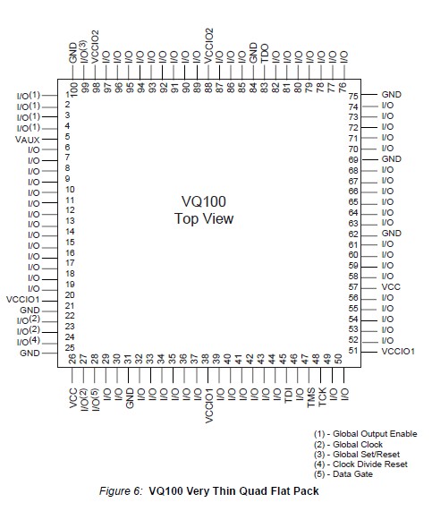
The XC2C256-7VQG100I is a CPLD. The XC2C256-7VQG100I is designed for both high performance and low power applications. This lends power savings to high-end communication equipment and high speed to battery operated devices. Due to the low power stand-by and dynamic operation, overall system reliability is improved. The XC2C256-7VQG100I consists of sixteen Function Blocks inter-connected by a low power Advanced Interconnect Matrix (AIM). The AIM feeds 40 true and complement inputs to each Function Block. The Function Blocks of the XC2C256-7VQG100I consist of a 40 by 56 P-term PLA and 16 macrocells which contain numerous configuration bits that allow for combinational or registered modes of operation.
Parametrics
XC2C256-7VQG100I absolute maximum ratings: (1)VCC, Supply voltage relative to ground: –0.5 to 2.0 V; (2)VCCIO, Supply voltage for output drivers: –0.5 to 4.0 V; (3)VJTAG, JTAG input voltage limits: –0.5 to 4.0 V; (4)VAUX, JTAG input supply voltage: –0.5 to 4.0 V; (5)VIN, Input voltage relative to ground: –0.5 to 4.0 V; (6)VTS, Voltage applied to 3-state output: –0.5 to 4.0 V; (7)TSTG, Storage Temperature (ambient): –65 to +150℃; (8)TJ, Junction Temperature: +150℃.
Features
XC2C256-7VQG100I features: (1)Optimized for 1.8V systems:As fast as 5.7 ns pin-to-pin delays; As low as 13 μA quiescent current; (2)Industry’s best 0.18 micron CMOS CPLD: Optimized architecture for effective logic synthesis; refer to the CoolRunner-II family data sheet for architecture description; Multi-voltage I/O operation — 1.5V to 3.3V; (3)Available in multiple package options: 100-pin VQFP with 80 user I/O;144-pin TQFP with 118 user I/O;132-ball CP (0.5mm) BGA with 106 user I/O;208-pin PQFP with 173 user I/O;256-ball FT (1.0mm) BGA with 184 user I/O;Pb-free available for all packages; (4)Advanced system features: Fastest in system programming:1.8V ISP using IEEE 1532 (JTAG) interface; IEEE1149.1 JTAG Boundary Scan Test; Optional Schmitt-trigger input (per pin); Unsurpassed low power management: DataGATE enable (DGE) signal control; Two separate I/O banks; RealDigital 100% CMOS product term generation; Flexible clocking modes.
Diagrams
| Image | Part No | Mfg | Description |  |
Pricing (USD) |
Quantity | ||||||||||
|---|---|---|---|---|---|---|---|---|---|---|---|---|---|---|---|---|
 |
 XC2C256-7VQG100I |
|
IC CR-II CPLD 256MCELL 100-VQFP |
Data Sheet |
|
|
||||||||||
| Image | Part No | Mfg | Description | |
Pricing (USD) |
Quantity | ||||||||||
 |
XC2C32A-4CPG56C |
|
IC CPLD 32MCELL 21 I/O 56-CSBGA |
Data Sheet |
|
|
||||||||||
|
XC2C32A-4QFG32C |
|
IC CR-II CPLD 32MCELL 32-QFN |
Data Sheet |
|
|
||||||||||
|
XC2C32A-4VQG44C |
|
IC CPLD 32MCELL 21 I/O 44-VQFP |
Data Sheet |
|
|
||||||||||
|
XC2C32A-6CPG56C |
|
IC CR-II CPLD 32MCELL 56-BGA |
Data Sheet |
|
|
||||||||||
|
XC2C32A-6CPG56I |
|
IC CR-II CPLD 32MCELL 56-CSBGA |
Data Sheet |
|
|
||||||||||
|
XC2C256-7TQG144C |
|
IC CR-II CPLD 256MCELL 144-QFP |
Data Sheet |
|
|
||||||||||